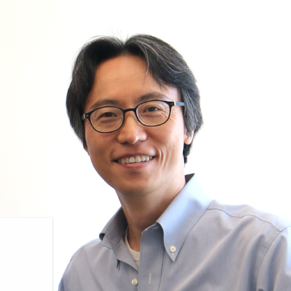
The Park group research focuses on the science and technology of precisely engineered nanomaterials. Our research is multidisciplinary; the group includes researchers with diverse backgrounds, including chemistry, physics, material science, and electrical engineering.
One of our main research goals is to build atomically-thin integrated circuitry. For this, we develop advanced growth, characterization and device fabrication methods for 2D layered materials, which include electrically conducting graphene, insulating hBN and semiconducting transition metal dichalcogenides. For example, we reported the metal-organic chemical vapor deposition (MOCVD) growth of wafer-scale three-atom-thick semiconductor MoS2 and WS2 films with high mobility (Nature, 2015) and developed a method for producing atomically thin lateral heterojuctions within individual 2D films based on graphene/hBN (Nature, 2012) and coherent lateral superlattices based on WS2/WSe2 (Science, 2018). We also showed that these monolayer films can be stacked vertically to form large-scale vertical superlattice and heterojunction films with atomic precision (Nature, 2017). More recently, we extended our synthesis and processing capability using novel synthesis and transfer of 2D polymers based on metal- and covalent-organic frameworks (Science, 2019). These 2D materials and structures are studied using advanced characterization methods including transmission electron microscope (TEM) (Nature, 2011; Nature, 2018) and spatially-resolved electrical measurements (Science, 2012). Our results enable the fabrication of electrically isolated active and passive elements embedded in continuous, one- and few-atom-thick sheets, which could further be manipulated and stacked to form complex devices at the ultimate thickness limit.
Another research goal is to explore novel electrical, optical, thermal, and mechanical properties of low-dimensional (1D & 2D) nanostructures, which will allow the development of advanced devices, including highly efficient solar cells, ultrasensitive infrared bolometric detectors, and novel valleytronic and spintronic devices. For example, we reported giant circular dichroism (Nature Nanotech. 2016) in graphene and the valley Hall effect in MoS2 transistors (Science, 2014).More recently, we reported the world’s most anisotropic thermal conductors produced based on stacked 2D materials(Nature, 2021) and three-atom thick optical waveguides, named “delta-waveguides” (Science, 2023) based on monolayer MoS2.
Seoul National University
B.S.
1996
UC Berkeley
Ph.D.
2003
Rowland Institute, Harvard University
Junior Fellow
2006
Cornell University
Assistant Professor
2012
Cornell University
Associate Professor
2016
The University of Chicago
Professor
Present
M. Lee, H. Hong, J. Yu, F. Mujid, A. Ye, C. Liang, and J. Park, “Wafer-scale δ-waveguides for integrated two-dimensional photonics”, Science, 381, 648-653 (2023).
S. E. Kim, F. Mujid, A. Rai, F. Eriksson, J. Suh, P. Poddar, A. Ray, C. Park, E. Fransson, Y. Zhong, D. A. Muller, P. Erhart, D. G. Cahill, and J. Park, “Extremely anisotropic van der Waals thermal conductors”, Nature, 597, 660-665 (2021).
Y. Zhong, B. Cheng, C. Park, A. Ray, S. Brown, F. Mujid, J.-U. Lee, H. Zhou, J. Suh, K.-H. Lee, A. J. Mannix, K. Kang, S. J. Sibener, D. A. Muller and J. Park, “Wafer-scale synthesis of monolayer two-dimensional porphyrin polymers for hybrid superlattices”, Science, 366, 1379-1384 (2019).
Y. Jiang, Z. Chen, Y. Han, P. Deb, H. Gao, S. Xie, J. Park, V. Elser, P. Purohit, M. W. Tate, S. Gruner, D. A. Muller, “Electron ptychography of 2D materials to deep sub-ångström resolution”, Nature, 559, 343-349 (2018).
S. Xie, L. Tu, Y. Han, L. Huang, K. Kang, K. U. Lao, P. Poddar, C. Park, D. A. Muller, R. A. DiStasio Jr., and J. Park, “Coherent, Atomically-Thin Transition-Metal Dichalcogenide Superlattices with Engineered Strain”, Science, 359, 1131-1136 (2018).
K. Kang, K.-H. Lee, Y. Han, H. Gao, S. Xie, D. A. Muller, and J. Park, “Layer-by-layer assembly of two-dimensional materials into wafer-scale heterostructures,” Nature, 550, 229-233 (2017).
C.-J. Kim, A. Sanchez-Castillo, Z. Ziegler, Y. Ogawa, C. Noguez, and J. Park, “Chiralatomically thin films,” Nature Nanotechnology, 11, 520-524 (2016).
K. Kang, S. Xie, L. Huang, Y. Han, P. Y. Huang, K. F. Mak, C.-J. Kim, D. A. Muller, andJ. Park, “High-performance three-atom-thick semiconducting films with wafer scale homogeneity,” Nature, 520, 656-660 (2015).
K. F. Mak, K. L. McGill, J. Park and P. L. McEuen, “The Valley Hall Effect in MoS2 Transistors”, Science, 344, 1489-1492 (2014).
M. P. Levendorf, C.-J. Kim, L. Brown, P. Y. Huang, R. W. Havener, D. A. Muller, and J.Park, “Graphene and Boron Nitride Lateral Heterostructures for Atomically Thin Circuitry”, Nature, 488, 627-632 (2012).
A. W. Tsen, L. Brown, M. P. Levendorf, F. Ghahari, P. Y. Huang, C. S. Ruiz-Vargas, R. W.Havener, D. A. Muller, P. Kim, and J. Park, "Tailoring Electrical Transport across Grain Boundaries in Polycrystalline Graphene", Science, 336, 1143-1146 (2012).
P. Y. Huang, C. S. Ruiz-Vargas, A. M. van der Zande, W. S. Whitney, M. P. Levendorf, J.W. Kevek, S. Garg, J. S. Alden, C. J. Hustedt, Y. Zhu, J. Park, P. L. McEuen, and D. A. Muller, “Grains and Grain Boundaries in Single-Layer Graphene Atomic Patchwork Quilts,” Nature, 469, 389-392 (2011).
Scientist of the Year, Korean Federation of Science and Technology Societies
2023
APS Fellow
2022
Dreyfus Foundation Postdoctoral Program Award
2017
Alfred P. Sloan Research Fellow
2010
Presidential Early Career Award for Scientists and Engineers
2009
National Science Foundation CAREER Award
2008
Rowland Junior Fellow, Harvard University
2003 - 2006
University of Chicago scientists invent smallest known way to guide light
Jiwoong Park Named Next Chair of Chemistry Department
Chuan He, Wenbin Lin, and Jiwoong Park recognized as Clarivate 2022 Highly Cited Researchers
